 PDF(2456 KB)

200 V All-SiC Integration Technology
GU Yong, MA Jie, LIU Ao, HUANG Run-hua, LIU Si-yang, BAI Song, ZHANG Long, SUN Wei-feng
ACTA ELECTRONICA SINICA ›› 2024, Vol. 52 ›› Issue (7) : 2183-2189.
PDF(2456 KB)
PDF(2456 KB)
200 V All-SiC Integration Technology
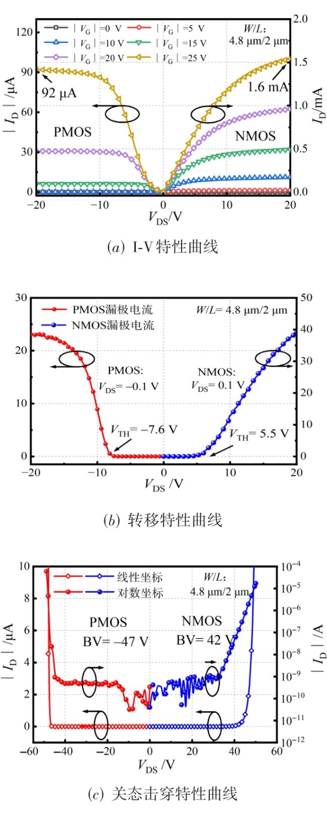
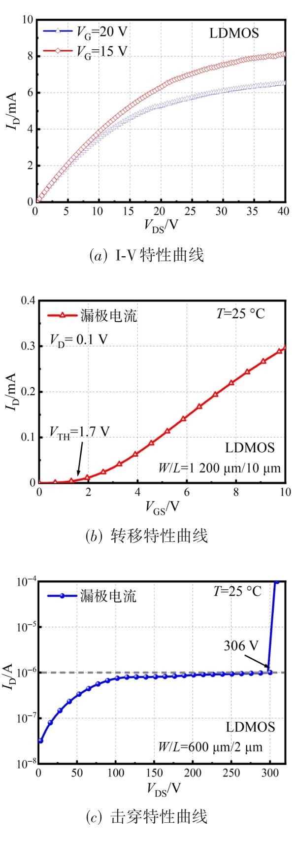
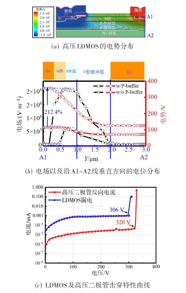
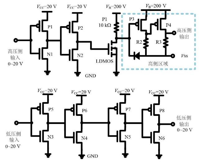
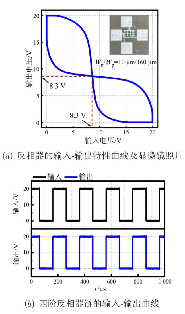
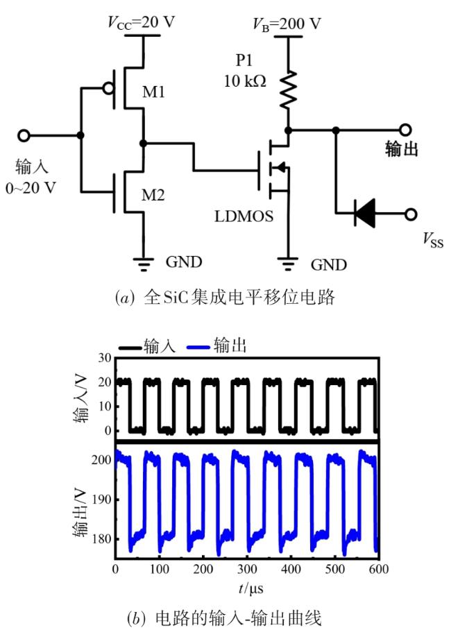
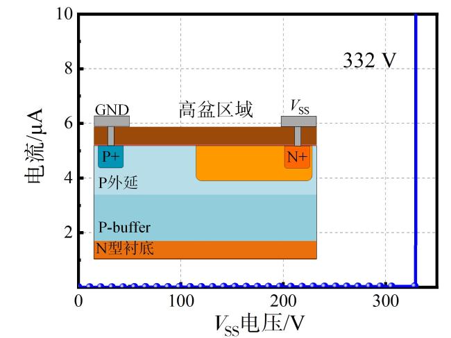
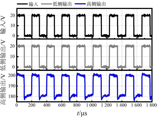
An all silicon carbide integrated process platform based on the wafer with N-substrate and P-epitaxy is proposed in this paper, which is compatible with CMOS (Complementary Metal Oxide Semiconductor field-effect transistor) devices, LDMOS (Laterally-Diffused MOS) and high-voltage diodes. A P-buffer layer is adopted to modulate the vertically distributed electric field and potential, which results in 212.4% improvement in vertical voltage withstanding. The LDMOS, high voltage diode and high side region can achieve more than 300 V breakdown voltage in 2 μm P-type epitaxial layer. Based on this platform, SiC (Silicon Carbide) CMOS inverter and inverter chain are constructed, all of which achieve voltage output ranging from 0~20 V with rail-to-rail capability. A half-bridge driving circuit is designed with a four-stage inverter chain as the low-side driver circuit. The high-side driver circuit consists of level-shifting circuit and a high-side region inverter chain circuit, producing an output of 180~200 V floating gate drive signal.
silicon carbide (SiC) / integration / silicon carbide integrated circuit / SiC inverter / SiC laterally-diffused metal Oxide semiconductor {{custom_keyword}} /
表1 全SiC集成工艺参数 |
| 参数 | 数值 |
|---|---|
| 衬底浓度 | 7.0×1018 cm-3 |
| P型缓冲层厚度 | 1.0 μm |
| P型缓冲层浓度 | 1.0×1017 cm-3 |
| P型外延层厚度 | 1.0 μm |
| P型外延层浓度 | 1.0×1016 cm-3 |
| LDMOS沟道长度 | 1.7 μm |
| 栅氧厚度 | 450 Å |
| N阱浓度 | 4.0×1012 cm-2 |
| LDMOS漂移区长度 | 10 μm |
| 多晶硅掺杂浓度 | 1.0×1019 cm-3 |
| 1 |
{{custom_citation.content}}
{{custom_citation.annotation}}
|
| 2 |
{{custom_citation.content}}
{{custom_citation.annotation}}
|
| 3 |
何其恢, 朱立东. 一种基于双图案的卫星信号能量检测粗同步方法[J]. 电子学报, 2022, 50(3): 524-532.
{{custom_citation.content}}
{{custom_citation.annotation}}
|
| 4 |
{{custom_citation.content}}
{{custom_citation.annotation}}
|
| 5 |
{{custom_citation.content}}
{{custom_citation.annotation}}
|
| 6 |
{{custom_citation.content}}
{{custom_citation.annotation}}
|
| 7 |
{{custom_citation.content}}
{{custom_citation.annotation}}
|
| 8 |
{{custom_citation.content}}
{{custom_citation.annotation}}
|
| 9 |
{{custom_citation.content}}
{{custom_citation.annotation}}
|
| 10 |
周郁明, 穆世路, 杨华, 等. Si/SiC混合开关最优门极延时及其在逆变器中的应用[J]. 电子学报, 2023, 51(6): 1468-1473.
{{custom_citation.content}}
{{custom_citation.annotation}}
|
| 11 |
{{custom_citation.content}}
{{custom_citation.annotation}}
|
| 12 |
{{custom_citation.content}}
{{custom_citation.annotation}}
|
| 13 |
{{custom_citation.content}}
{{custom_citation.annotation}}
|
| 14 |
{{custom_citation.content}}
{{custom_citation.annotation}}
|
| {{custom_ref.label}} |
{{custom_citation.content}}
{{custom_citation.annotation}}
|


 PDF(2456 KB)
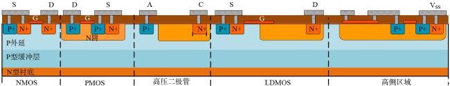
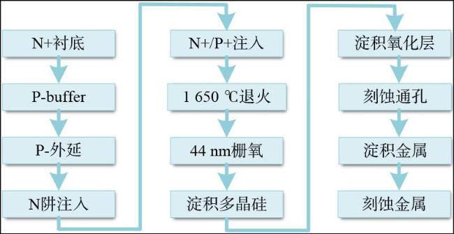
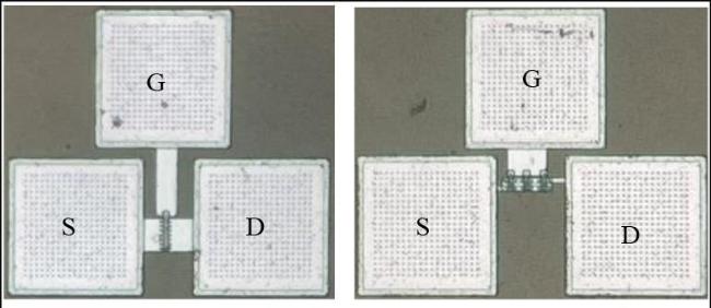
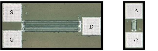
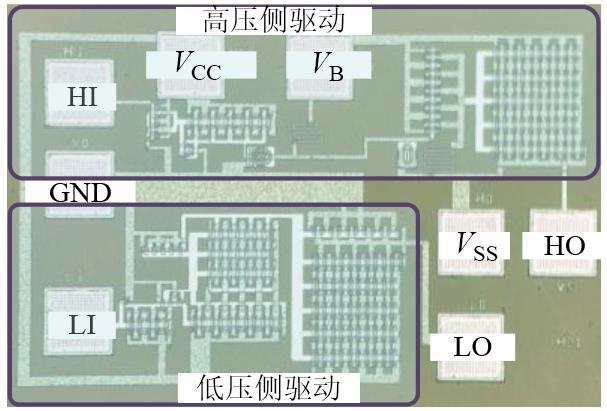
 图1 全SiC集成工艺剖面结构示意图图2 全SiC集成关键步骤
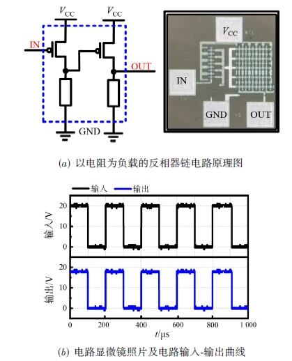
 表1 全SiC集成工艺参数图3 器件显微镜照片图4 NMOS和PMOS的特性曲线对比图5 LDMOS直条状版图布局显微镜照片图6 LDMOS的电学特性曲线图7 高压器件电势优化图8 SiC全集成半桥驱动电路图图9 反相器及反相器链输出特性图10 电平移位电路及其输出特性图11 高测区域隔离结构击穿电压图12 电阻负载的反相器链及其输出特性图13 全SiC集成半桥驱动电路芯片表面显微镜照片图14 全SiC集成半桥驱动电路输入输出曲线
/
| 〈 |
|
〉 |


